Understanding the PCB Design Process: A Step-by-Step Guide
Printed Circuit Boards (PCBs) play a crucial role in modern electronics, acting as the foundation for almost every electronic device. Whether you're a beginner or exploring electronics design, understanding how PCB design works is essential. This guide breaks down the process into simple, easy-to-follow steps. If you want to excel in this career path, then it is recommended that you upgrade your skills and knowledge regularly with the latest PCB Design Course in Bangalore.
What Does PCB Design Mean?
PCB design is the process of developing a structured layout that connects electronic components like resistors, capacitors, and integrated circuits on a board. The aim is to ensure smooth electrical operation while meeting design and manufacturing standards.
Stages Involved in PCB Design
1. Creating the Schematic
The process starts with a schematic diagram, which represents the logical connections of the circuit.
Main activities:
- Choosing the required components
- Organizing them based on their roles
- Linking them using virtual connections
2. Selecting Components
Picking suitable components directly impacts the performance of the PCB.
Key considerations:
- Electrical ratings such as voltage and current
- Physical size and packaging
- Cost and availability in the market
- Reliability under operating conditions
3. Designing the Layout
At this stage, the schematic is transformed into a physical PCB structure.
This step includes:
- Placing components efficiently on the board
- Managing space for compact design
- Ensuring proper alignment with mechanical constraints
It’s simpler to master this tool and progress your profession with the help of PCB Design Training which provide thorough instruction and job placement support to anyone seeking to improve their talents.
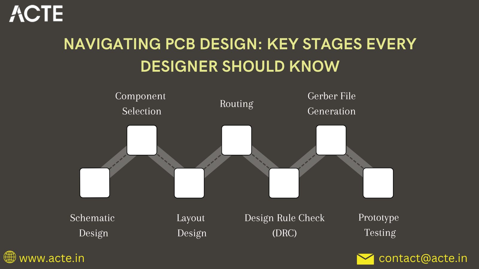
4. Connecting the Circuit (Routing)
Routing involves creating conductive paths (traces) to connect components.
Important points:
- Choosing proper trace width for current flow
- Keeping traces short for better performance
- Reducing interference and signal noise
5. Running Design Checks (DRC)
Before manufacturing, the design must be verified through Design Rule Checks.
This ensures:
- Proper spacing and trace dimensions
- Correct electrical connections
- Compliance with fabrication standards
6. Preparing Manufacturing Files
After validation, design files (Gerber files) are generated for production.
These files include:
- Details of PCB layers
- Drilling information
- Component positioning
7. Testing the Prototype
A prototype is created to test the real-world performance of the PCB.
Testing helps to:
- Detect and fix design errors
- Verify functionality
- Improve the design before mass production
Final Thoughts
PCB design requires attention to detail and a structured approach. By following each stage carefully—from schematic creation to prototype testing—you can develop efficient and reliable circuit boards.
As electronics continue to evolve, gaining expertise in PCB design will open up many opportunities in the technology field. Continuous learning and practice are key to mastering this skill.